
Full ODM 5G & LTE Hardware Development Supplier
End-to-end custom wireless hardware development: industrial design, PCB schematic layout, Qualcomm/MediaTek chipset integration, carrier lab pre-certification, and high-volume SMT manufacturing.
Development Scope
Turnkey ID/PCB
Full mechanical & baseband
Silicon Platforms
Qualcomm / MTK
Tier-1 enterprise chipsets
Carrier Testing
PTCRB & Lab
Pre-compliance testing
IP Protection
Strict NDA
Client owns tooling & design
Turnkey Wireless Hardware Engineering & SMT Manufacturing Under One Roof
The AceTel Full ODM Hardware Development Program (Tier 3) is a comprehensive product realization partnership engineered for tier-1 telecom operators, industrial automation conglomerates, smart-city contractors, and defense/public safety organizations requiring proprietary hardware that cannot be solved by off-the-shelf catalog products.
As a dedicated LTE router ODM supplier and 5G CPE ODM manufacturer, AceTel integrates the entire hardware lifecycle under one ISO 9001:2015 certified roof — spanning industrial design (ID), mechanical thermal engineering (MD), high-speed multi-layer PCB layout, baseband RF design, customized OpenWrt BSP development, regulatory type approvals, and high-precision SMT manufacturing in our Shanghai facility.
Full-Stack In-House Engineering Capabilities
Our cross-disciplinary R&D team bridges silicon-level radio frequency design with ruggedized mass-production manufacturing:
1. Industrial Design (ID) & Mechanical Thermal Modeling
- Form Factor Tailoring: Custom form factors including low-profile DIN-rail enclosures, pole-mount IP67/IP68 outdoor weatherproof casings, and sleek enterprise desktop designs.
- Thermal Simulation & Dissipation: Computational Fluid Dynamics (CFD) thermal modeling ensuring passive cooling stability for high-power 5G sub-6 GHz and mmWave radio modules in harsh ambient environments (-40°C to +85°C).
- Tooling & Mold Fabrication: High-precision CNC steel molds for ABS/PC flame-retardant plastics and die-cast aluminum alloy chassis.
2. High-Speed PCB Layout & RF Baseband Engineering
- Multi-Layer High-Density Interconnect (HDI): Design of 8-to-14 layer high-speed PCBs with impedance control, signal integrity (SI) simulation, and power distribution network (PDN) optimization.
- RF & Antenna Engineering: Custom 4x4 and 8x8 MIMO internal antenna array design, active GPS/GNSS receiver integration, and 3D radiation pattern tuning inside our in-house RF anechoic chambers.
- Specialized Industrial Interfaces: Hardware-isolated RS232/RS485 terminal blocks, CAN-bus vehicle interfaces, M12 ruggedized Ethernet connectors, PoE++ (802.3bt) power input, and multi-SIM active failover circuitry.
3. Silicon Architecture & Chipset Alliances
- Qualcomm Snapdragon Platforms: Enterprise-tier 5G NR basebands (Snapdragon X62, X55) paired with multi-core networking processors (IPQ5018 / IPQ8072).
- MediaTek Platforms: High-throughput 5G FWA platforms (T750) and dual-band Wi-Fi 6/7 Filogic chipsets.
- UNISOC & Realtek Platforms: Value-optimized LTE Cat 1, Cat 4, and Cat 7 baseband architectures for high-volume IoT telemetry and cost-sensitive utility deployments.
4. Regulatory & Carrier Lab Pre-Compliance Testing
- In-House Testing Infrastructure: Multi-point environmental thermal cycling, vibration tables, ESD air/contact discharge testing, and conducted RF emissions.
- Global Compliance Package: Turnkey handling of CE (RED), FCC Part 15/90/96 (CBRS), PTCRB, GCF, RoHS, REACH, and WEEE certifications.
The ODM Product Realization Roadmap
We guide your custom wireless hardware project through a disciplined 6-stage Stage-Gate engineering methodology:
| Phase | Duration | Core Engineering Milestones & Deliverables |
|---|---|---|
| Phase 1: Architecture & Feasibility | Weeks 1–3 | Detailed PRD review, BOM component selection, preliminary cost modeling, industrial styling concepts. |
| Phase 2: Industrial & Mechanical Design | Weeks 4–7 | 3D CAD modeling, thermal CFD simulation, rapid SLA prototyping, mechanical fit verification. |
| Phase 3: EVT (Engineering Verification) | Weeks 8–14 | PCB schematics, multi-layer Gerber layout, tooling kick-off, first 10–20 working PCBA prototypes. |
| Phase 4: DVT (Design Verification) | Weeks 15–20 | Tooling trial parts (T0/T1), firmware bring-up, RF tuning, pre-compliance anechoic testing. |
| Phase 5: PVT (Production Validation) | Weeks 21–26 | Pilot run on mass-production SMT lines, test fixture validation, formal CE/FCC/PTCRB submissions. |
| Phase 6: MP (Mass Production & NPI) | Week 27+ | High-volume automated assembly, AOI inspection, automated RF calibration, and global logistics hand-off. |
IP Protection, Tooling Ownership & Manufacturing Guarantees
- Guaranteed Tooling Ownership: You retain 100% legal ownership of all dedicated injection molds, stamping dies, and custom test fixtures upon project completion.
- Strict Confidentiality Protocols: Segregated engineering data environments, dedicated project repositories, and strict mutual NDAs protecting your competitive advantage.
- Component Lifecycle Protection: Proactive Product Change Notifications (PCN) and End-of-Life (EOL) management, guaranteeing 5 to 7 years of sustained component supply for enterprise deployments.
- Scalable Shanghai SMT Capacity: Multi-line surface-mount manufacturing with automated solder paste inspection (SPI), automated optical inspection (AOI), and in-circuit testing (ICT).
Compatible Hardware Platforms Available Immediately
These pre-certified cellular platforms can be white-labeled, custom-firmwared, or used as the foundational baseline for your ODM hardware program.
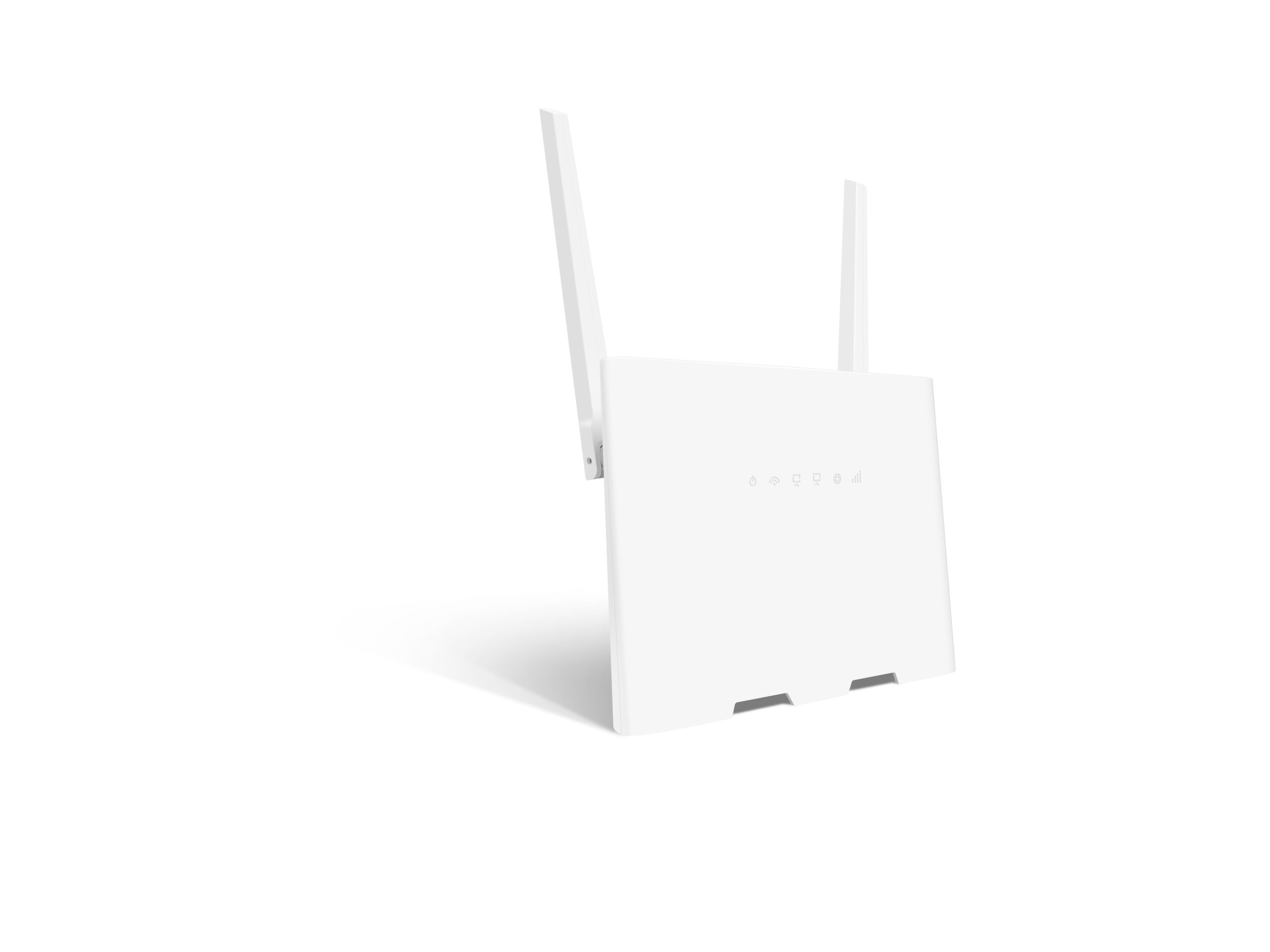
AceTel R1260S 4G LTE Cat6 CPE Router
LTE-Advanced Cat6 Baseband + Gigabit Wi-Fi Platform
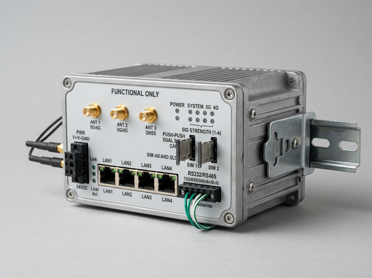
AceTel R310F Industrial 5G Router (WiFi 6, Dual SIM)
Qualcomm 64-bit Dual-Core ARM Processor (256MB DDR4 / 256MB Flash)
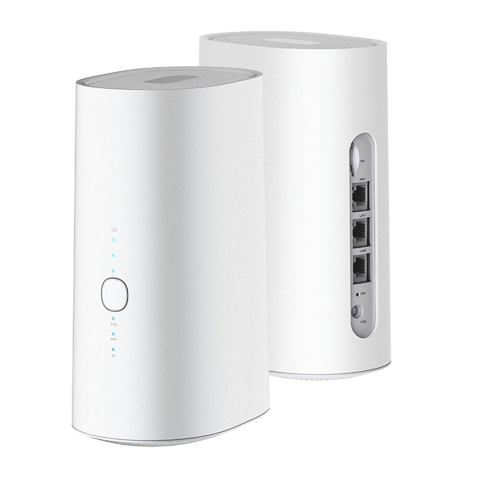
AceTel R5089 5G CPE Router (WiFi 6)
Qualcomm IPQ8072A + QCN5054 + QCN5024, Snapdragon X55/X65/X75 5G modem
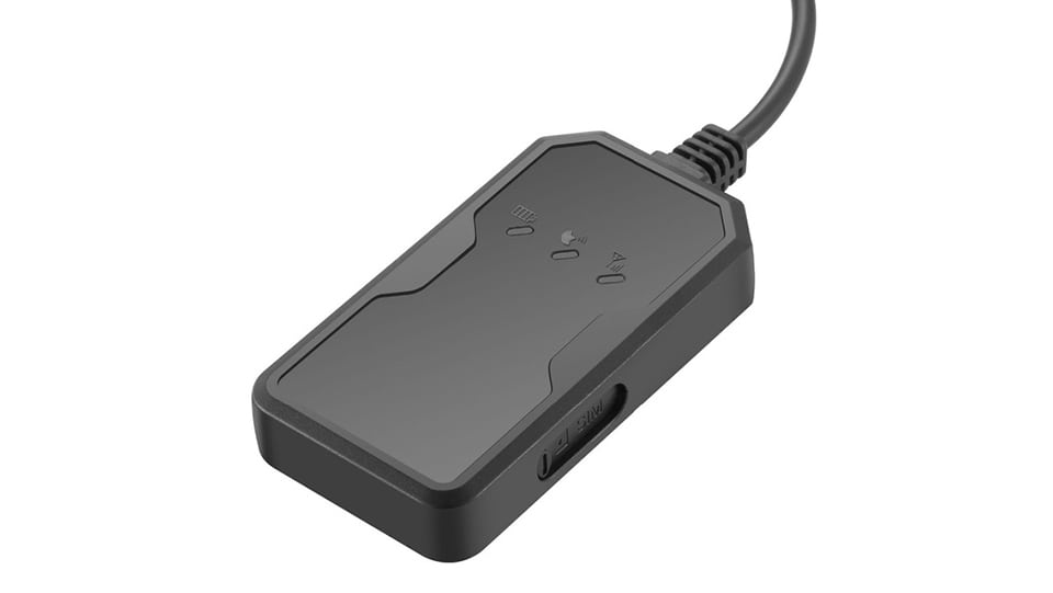
AceTel T810 4G LTE Cat-1 Commercial Vehicle GPS Tracker
Qualcomm MDM9207-1 (ARM Cortex-A7 @ 1.2 GHz) + Automotive MCU
Frequently Asked Questions
Key commercial, technical, and compliance inquiries regarding our Full Custom ODM Hardware Engineering.
- How does AceTel protect client intellectual property (IP) and custom hardware designs?
- We execute strict, binding Mutual Non-Disclosure Agreements (NDAs) prior to any engineering disclosures. Under our Full ODM agreement, all custom tooling, injection molds, PCB schematics, and mechanical CAD models are the exclusive intellectual property of the client.
- Who owns the injection molds and production tooling after NRE completion?
- The client owns 100% of all dedicated injection tooling, stamping dies, and specialized test fixtures. Upon project completion or request, tooling can be audited, transferred, or maintained under dedicated maintenance protocols in our clean-room facility.
- Which cellular baseband and processor platforms does AceTel engineer with?
- Our R&D team has deep architectural experience across tier-1 semiconductor platforms including Qualcomm Snapdragon X62/X55/IPQ5018, MediaTek T750/Filogic, Realtek, and UNISOC, enabling the right price-to-performance balance for your target deployment.
- Can AceTel manage carrier certification and regulatory testing (CE, FCC, PTCRB)?
- Yes, we provide complete turnkey certification management. We utilize in-house anechoic chambers and RF simulation for pre-compliance, then manage full testing and certification through accredited test houses for CE (RED), FCC, PTCRB, GCF, and operator-specific network lab acceptance.
- What is the typical timeline and NRE cost structure for ground-up ODM development?
- Typical ground-up ODM projects span 4 to 7 months from industrial design concepts to mass-production pilot runs (EVT/DVT/PVT/MP). NRE tooling and engineering costs are milestone-based, with flexible amortization options available against mass production volume commitments.
Request a Quote for Full ODM 5G & LTE Hardware Development Supplier
Tell us your target quantity, destination market and customization needs. Our sales engineers reply within 24 hours with pricing, MOQ options and lead time.